Gigapixel camera and chip mosaic
Gigapixel camera is increasingly recognized as the ultimate solution for imaging a very large field of view (FOV) with high spatial/angular resolution in recent years. In order to achieve this inaccessible requirement, optical systems need to be extended and elaborately designed for the outstanding performance over the whole FOV. Besides, another challenge for gigapixel camera is that there is no single photo-sensitive chip large enough to cover the entire FOV so far, and instead, a more feasible solution is to mosaic many smaller size (10~20 Megapixel) chips.
Chip mosaic generally has two approaches. One is to share a large objective lens and package all the chips following the back focal plane of the lens to individually re-image a sub-region of FOV. This approach was named as the inner-path mosaic, and researchers from Duke University and University of Arizona have proposed a practical implementation following this approach [D. J. Brady, Nature 2012]. As shown in Fig.1, by customizing a monocentric objective lens with all spherical surfaces, a spherical focal surface has been formed. In their system, 98 telecentric microcameras have been mounted in the pre-defined arrangement such that every local image field can be recorded on the corresponding chip. Since the optical axis of each microcamera is designed to be normal to the focal surface, distances between two neighboring microcameras could disperse along the axis to avoid spatial interference. However, there are some obvious drawbacks of the inner-path mosaic approach; for instance, complexities in the spherical image mosaic, load and dimensions explosion towards the pixel number, and dependence on the special optical system design and fabrication.
Another chip mosaic approach is to duplicate four image systems with the same performances and arrange chips into a sparse array at image plane, respectively, which was named as outer-path mosaic. Generally, duty cycle as 50% will be appropriate for the most 2D chip mosaic, because the packaging area is less than photo-sensitive area on the chip.
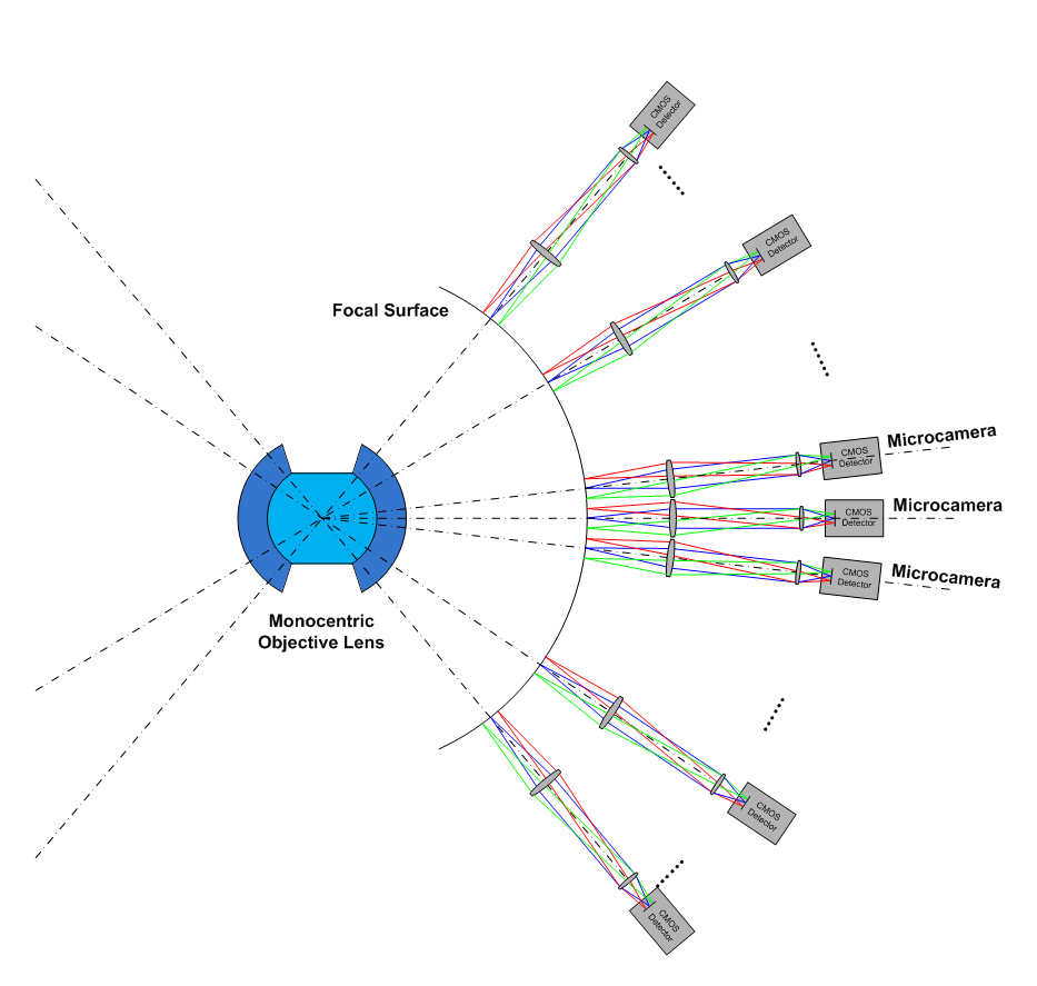
Fig.1 Gigapixel camera schematic in inner-path mosaic [D. J. Brady, Nature 2012]
Our Gigapixel Camera implementation (2014-2016)
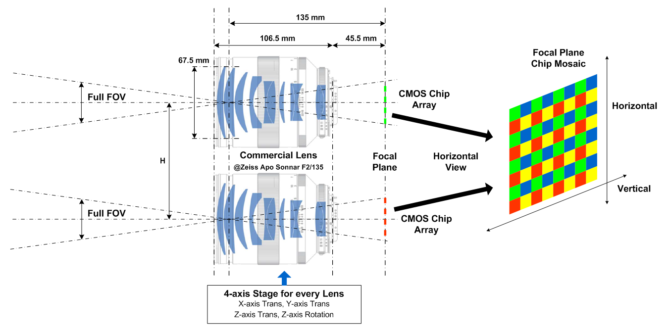
(a) Our gigapixel camera schematic (horizontal view) in outer-path mosaic.
(b) Idealized object-image plane in outer-path mosaic.
Fig.2 Schematic of our gigapixel camera (horizontal view).
In order to overcome above drawbacks in inner-path mosaic and simplify the alignment and mosaic processing on image plane, I have proposed an alternative gigapixel camera in outer-path mosaic, as illustrated in Fig.2. Basing on four high quality fixed focal length lenses (Zeiss, Apo Sonnar F2/135mm), 64 CMOS chips (Sony IMX 135, 4208×3120, 1.12um/pixel, 24fps@full frame) were integrated to mosaic 0.8 Gigapixel image over the Full Frame (15.6°×10.5°, 36×24mm). As the maximum F# of Lens is 2, the diffraction limit of these lenses is around 600nm, which is half of the pixel pitch.
In our prototype system, I custom designed four functional and geometric equivalent PCB boards with 2x2 bare CMOS chips welded on each, as shown in Fig.3(a). The connections between PCB with their processing electronics use flexible printed circuit cable. The overall arrangement is illustrated in Fig.3(b) as well as the chip mosaic arrangement in Fig.3(c).
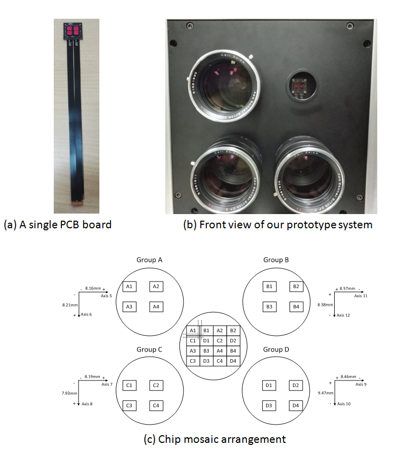
Fig.3 Front view of prototype system and chip arrangement.
Position for each of the four PCB boards could be easily adjusted by four-axis motorized translation and rotation stage. Two FPGA boards (Xlinx,KC705) are equipped to do the image grabbing and data transferring to workstation using two PCIe x8 Gen3 extension Cables (~2.5GB/s/cable) each measured 2m in length. Furthermore, real-time vignetting compensation, various geometric transforms (rotation, scaling, etc…), 2D image mosaic and real-time display, are processed by a GTX980 GPGPU.
For our outer-path mosaic, multiple misalignments among 16 chips and 4 groups need to be dealt with, for example, rotation errors, tip/tilt errors, scaling errors, and displacement errors. Besides, the chief ray angle (CRA) mechanism on every cell phone CMOS chip might cause the vignetting effect on the image. Moreover, due to the non-coaxial nature of four image systems, the relative positioning of all chips needs to be actively adjusted when working distance changes. Therefore, the offline calibration and online computational imaging have been carried out.
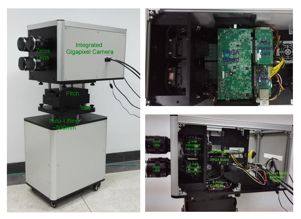
Fig.4 Integrated gigapixel camera prototype with 3-axis (Yaw, Pitch and Lifting) support.
Offline calibration (2016)
The offline calibration consists of image de-vignetting and rotation & scaling estimation.
[Image De-vignetting] In order to eliminate the vignetting from raw images on every chip, we used the gigapixel camera to take different color cards under the approximately uniform illumination, and different 16 vignetting images were acquired. Then we did polynomial surface fitting to the different spectral images, getting spectral distributions of vignette. From the polynomial distributions of vignette, we could compute the matrix of dodging coefficients which will be used in real-time de-vignetting processing.
[Rotation & Scaling Estimation] Without considering tip/tilt errors and displacement errors, we directly estimated the rotation and scaling errors between the 16 images basing on the forward model of affine transformation and integer position interpolation. In practice, interpolation would be unnecessary when 16 point-array patterns were presented in the object plane. For these binary images, we constructed the objective function not on the entire image but on the black points with their centroid positions:
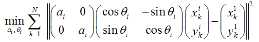
Quasi-Newton method has been used to obtain the solution of above optimization problem. Due to these rotation errors and scaling factors were intrinsic in the system, them could be used in real-time geometric correction processing, as shown in Fig.5.

Fig.5 Offline calibration result and corresponding corrections and 2D image mosaic.
Online computational imaging (2016-present)
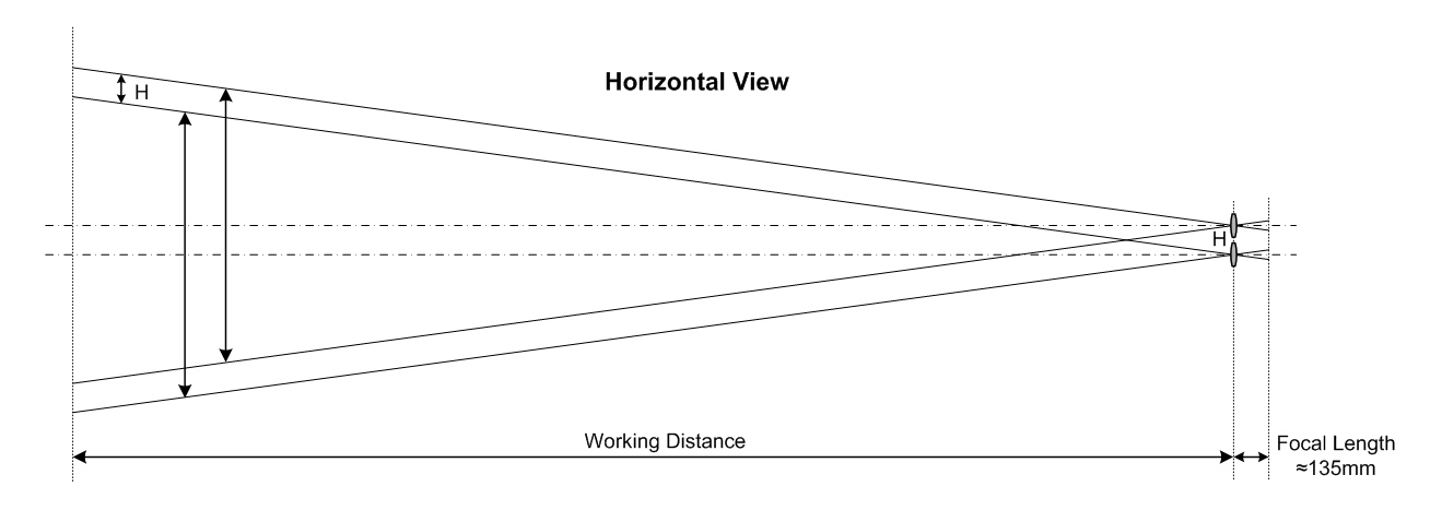
After offline calibration under the laboratory conditions, our prototype will move to outdoor. That means the working distance will dramatically increase. As illustrated in Fig.6, when the working distance is changed from  to
to  , chip positions on each board need to be correspondingly moved in principle. Here, only two upper horizontal lenses are taken into consideration, the actual distance between two optical axes in horizontal direction and vertical direction are labeled as
  and
and  , and the actual angle between two optical axes in horizontal direction and vertical direction are labeled
  as
as  .
.
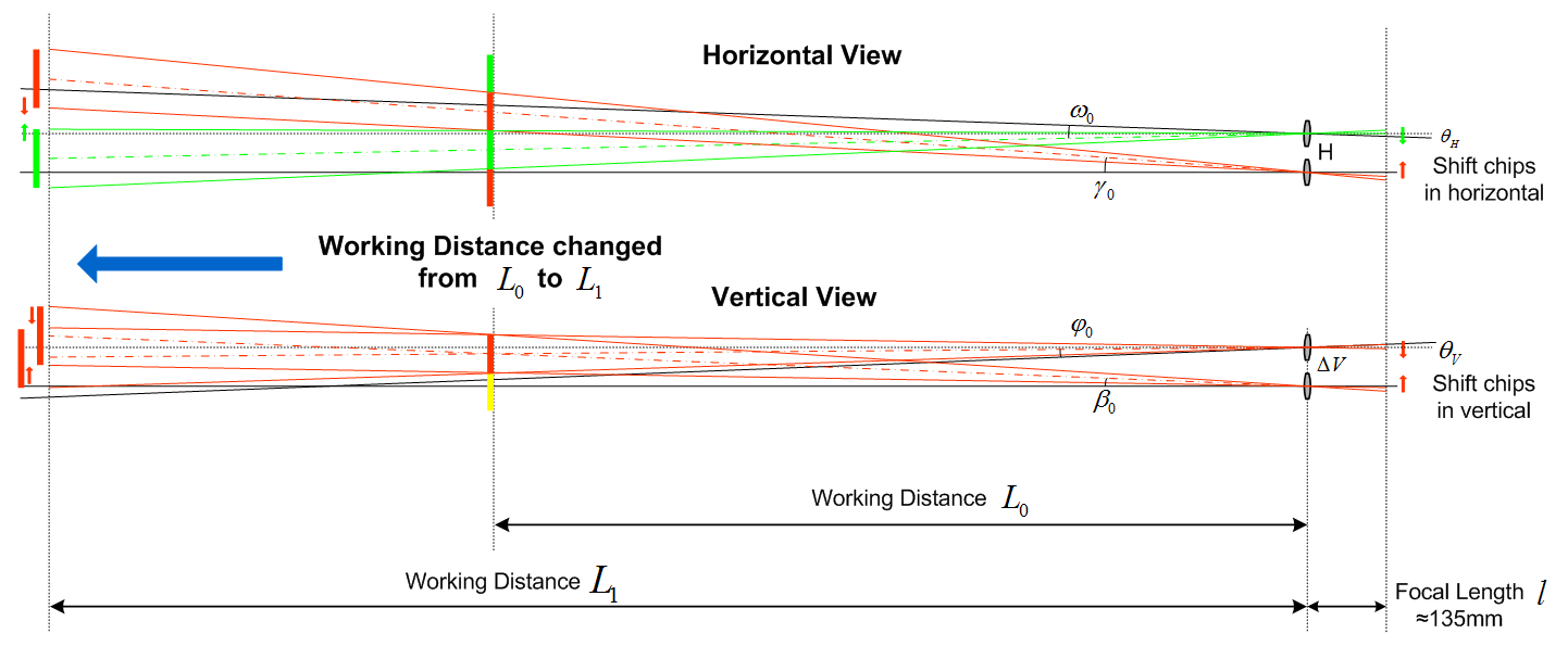
Fig.6 Chips move in principle on object plane and focal plane while working distance changes.
Basing on the geometric relationship, the horizontal shift in image plane will be
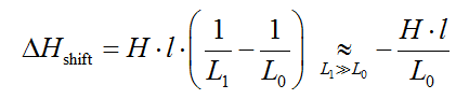
Similarly, the vertical shift in image plane will be
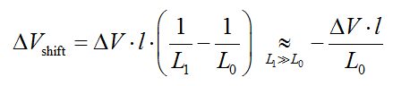
According to the above derivation, by quantitatively obtaining the  and
and  from motorized stage with high accurate grating at two known working distances, parameters and could be calibrated. As we seen that and were independent on the angular errors and between two optical axes, computational imaging could be possible for arbitrary working distance. During online computational imaging, automatic positioning compensation on each PCB board will execute once the working distance being sensed in changing. While the working distance becomes more than 1000m, these shifts will vary in few pixels which are much smaller than the overlap of two chips.
Current works
As demonstrated above, our property system will bring enormous potential to different applications of large FOV surveillance and remote sensing, apart from the advantage in compactness, low complexity, and simplicity in optical design.
[1] We are currently calibrating the distance errors between every two optical axes from four objective lenses. Four different working distances (5, 10, 20, and 40m) are considered into the calibration to fit the errors and validate the computational imaging.
[2] Evaluate the camera performances within long working distance, from 500 to 4000m.
Grants
[1] Investigator, Development and its application of super high-definition video real-time analysis and enhancement, Ministry of Science and Technology, Major Scientific Instrument Development, 2014-2019.
Patents
[1] Huizhu Jia, Heng Mao, Xiange Wen, Rui Chen, Xiaodong Xie, Wen Gao, A Large FOV Gigapixel Remote Camera and Imaging Method, Invention, No.201610773148.8, application date Aug 30, 2016.